Electronic Circuits - interfacing with a Z80 microprocessor v7 (output to I/O device)
My seb80 custom computer now has its own page here
This is version 7 of my Z80 interfacing project. My goal in this version was to introduce an I/O output device, which could receive data written to it via the OUT instruction.
Previous versions:
Previous versions:
- version 1 - initial wire-up, executes NOPs, observe incrementing address
- version 2 - experiment with and observe machine cycles M2 (memory read) and M3 (memory write)
- version 3 - address and data buses
- version 4 - introduce ROM and run program from it
- version 5 - introduce RAM
- version 6 - oscillator clock, NMI button, and INT/NMI tests
I made my first steps into I/O device interfacing. The test I/O output device I created consists of LEDs which display the last value written to the device's port.
The device's entry point is a 74LS373 octal d-type latch which snapshots the data bus when enabled. It is enabled by one of the outputs of a 74LS138 3-to-8 decoder, which serves as an output device selector.
The latch output is buffered by a 74LS244, which provides sufficient current for the LEDs.
See the log below for program listings.
TP4 - test program for I/O output
TP5 - increment-and-output test program for I/O
Log
day 1Began designing the I/O circuit. My plan is to expose selectors for eight different I/O devices via a 74LS138 3-to-8 decoder (part is SN74LS138N).
Wiring this up to A0-A2 will allow easy access to I/O ports 0 through 7.
For the prototyping stage (on the breadboard), I want to wire up and output device made up of 8 LEDs which will display the last value written to the respective I/O port.
I realized that by adding a second 74LS138 3-to-8 decoder I could expose 4 input and 4 output devices with no further chips.
One 74LS138 will rely on Z80's RD line to become enabled and the other will rely on Z80's WR line to become enabled.
Address line A2 will select between the first 4 and the next 4.
I/O devices at port 0, 1, 2, 3 (A2=0) will be input devices.
I/O devices at port 4, 5, 6, 7 (A2=1) will be output devices.
NOTE: for input devices that won't rely on these built-in selectors, care has to be taken that they are wired to ports whose A2=1, to not conflict with the built-in input device selectors which expect A2=0.
Output devices:
A2  A1  A0

C   B   A  Y

1   0   0  Y4  output device at port 4

1   0   1  Y5  output device at port 5

1   1   0  Y6  output device at port 6

1   1   1  Y7  output device at port 7
day 2
Wired the 74LS138 which will select between four output devices.
Wrote TP4, my first I/O output test program.
Address  Bytes                Mnemonic


0000                          ; TP4

0000                          ; test program for I/O output

0000                          ;

0000     3E 81                LD A, 10000001b

0002     D3 04                OUT (04h), A

0004     3E C3                LD A, 11000011b

0006     D3 05                OUT (05h), A

0008     3E E7                LD A, 11100111b

000A     D3 06                OUT (06h), A

000C     3E FF                LD A, 11111111b

000E     D3 07                OUT (07h), A

0010     C3 00 00             JP 0000h
Verified with a multimeter that the output device selector (74LS138) works as intended.
Since the main breadboard is running out of room, I've brought out the data lines onto a side breadboard.
Designed the first output device: 8 LEDs.
It's based on 74LS373 (part is DM74LS373N) octal d-type latch (transparent). While this latch has the advantage of having a level-sensitive LE (latch enable), it is active high, unlike all other TTL chips I've used so far. Luckily, my 74LS04 hex inverter still has some free slots.
The I/O output device selector was already tested, so all I had to do is connect a small breadboard which already had LEDs and a 74LS244 buffer wired up.
Wrote program TP5, below, which is supposed to successively write higher values to an output device, with visible delay. NMI should reset the value to 0.
Address  Bytes                  Mnemonic


0000                            ; TP5

0000                            ; second test program for I/O output

0000                            ;   increment value written to output port (with

0000                            ;   visible delay)

0000                            ;   NMI clears counter to zero

0000                            ;

0000     3E 00                  LD A, 0

0002     32 0F F0               LD (0F00Fh), A        ; counter := 0

0005                  MAIN_LOOP:

0005                            ; here, A = counter value

0005     D3 06                  OUT (06h), A          ; output counter value

0007     01 DE 08               LD BC, 2270           ; busy wait iteration count

000A                  DELAY:

000A     0B                     DEC BC                ; 4 clocks

000B     78                     LD A, B               ; 4 clocks

000C     B1                     OR C                  ; 4 clocks

000D                                                  ; (MSB OR LSB) = 0?

000D     C2 0A 00               JP NZ, DELAY          ; 10 clocks

0010                                                  ; no, keep looping

0010     21 0F F0               LD HL, 0F00Fh

0013     34                     INC (HL)

0014     3A 0F F0               LD A, (0F00Fh)

0017     C3 05 00               JP MAIN_LOOP

001A     FF FF ...              DB 76 DUP (0FFh)      ; pad up to NMI handler start

0066                  NMI_HANDLER:

0066     3E 00                  LD A, 0

0068     32 0F F0               LD (0F00Fh), A        ; counter := 0

006B     ED 45                  RETN                  ; return from NMI
The program ran successfully! The counter was observable on the LEDs of the output device and NMI successfully reset the counter to zero.
day 4
Updated diagram
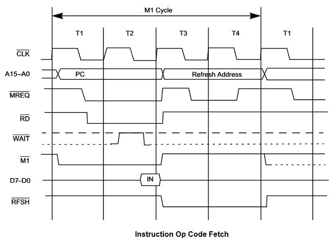
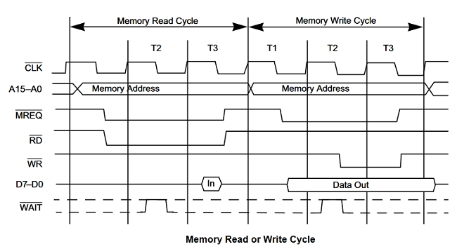
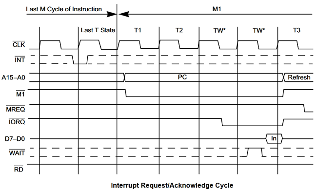
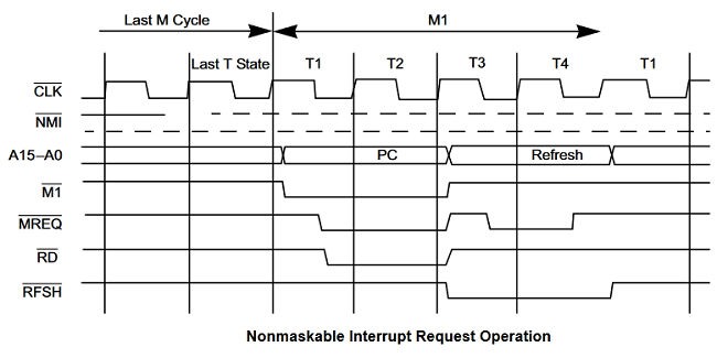
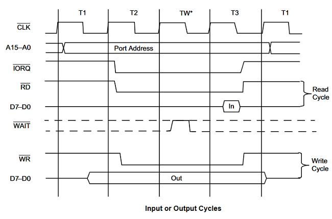
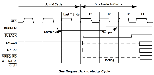
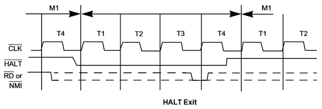
Z80 diagrams
Here are some useful diagrams, including the Z80 pinout, timing diagrams, etc.
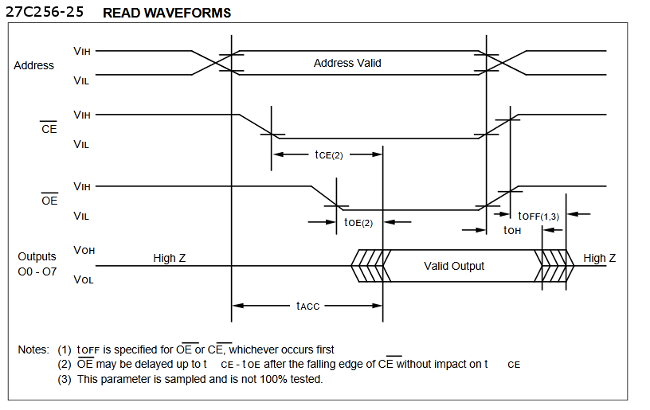
27C256 EPROM diagrams
Here are some useful diagrams, including pinout, timing, etc.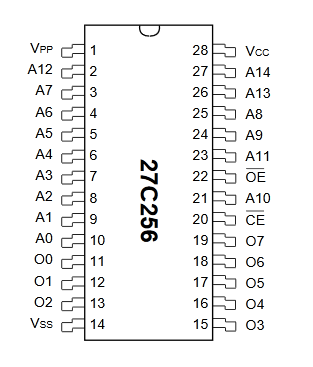
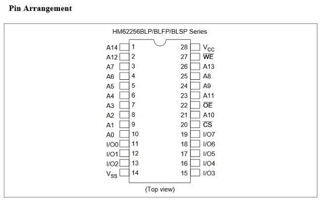
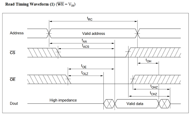
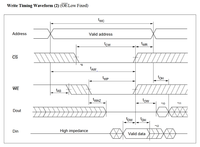
62256 RAM diagrams
Here are some useful diagrams, including pinout, timing, etc.