Electronic Circuits - interfacing with a Z80 microprocessor v5 (introduce RAM)
My seb80 custom computer now has its own page here
This is version 5 of my Z80 interfacing project. My goal in this version was to introduce RAM, as well as bring the RAM/ROM interfacing circuit to its final form.
Previous versions:
Previous versions:
Version 5 introduces RAM via the Hitachi HM62256LP-70 32kb RAM IC. Since both RAM and ROM are implemented via 32kb chips, no address decoding is necessary. Line A15 is used to switch between the two (low means ROM, high means RAM).
This maps memory addresses 0000-7FFF to ROM and 8000-FFFF to RAM.
To test my new setup, I've written a program which reads and writes (to RAM only) to the edges of RAM and ROM. I've asserted that the setup was valid by observing the data line LEDs as the Z80 read values from memory - and then comparing to my expectation.
See the log below for the program listing. You can also download the 32kb ROM binary here.
Log
day 1Validated my expectation that for IO writes, the Z80 keeps correct write data on its data lines past IORQ/WR returning to their inactive state.
This means that interfacing with D-type flip-flops should be reasonably easy.
My plan is to use them for a built-in, write-only device made up of 8 LEDs which I'll use for debugging, by simply OUTputting byte values (which get latched) to it.
day 2
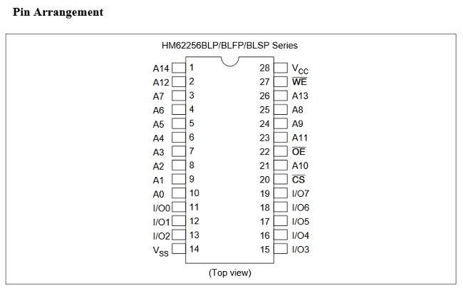
Started planning and diagramming the integration of the RAM chip. I'm using a Hitachi HM62256LP-70.
This is nice: the HM62256's pinout is very similar to the 27C256's.
By placing the RAM chip next to the ROM chip on the breadboard, I was able to bring address and data to the RAM chip neatly, using some very short jumper wires.
The RAM chip is fully wired up except for its control lines, which I still have to design.
I've hardwired its control (CS, OE, WE) high (inactive), so that I can still test that the ROM works well.
day 3
Designed final connections of data bus transceiver (74LS245) and settled on a chip select strategy.
Wired the 74LS245 transceiver to be enabled and disabled by the Z80, depending on MREQ and IORQ (when either becomes active). This was done simply with a 74LS08 AND gate.
Wired the 74LS245 transceiver to have its direction controlled by the Z80 via direct connection to Z80's RD line.
This many breadboards are dropping some voltage, so I've increase supply to 5.1V.
day 4
Designed the memory chip selection circuit. It will simply split on A15 between a 32k RAM chip and a 32k ROM chip.
This way all memory registers are uniquely addressable and all memory registers are addressable
For both RAM and ROM, OE (output enable) lines are connected directly to the RD line on the bus.
For RAM, WE (write enable) line is connected directly to the WR line on the bus.
To select one of RAM and ROM, I've used a 74LS139 1-of-4 decoder (also called 2-to-4). The exact part is DM74LS139.
The 74LS139 is enabled by Z80's MREQ. Its A input is tied to Z80's A15. Its B input is hardwired high.
day 5
Wired everything, moving previous connections to the ROM onto the decoder.
Ran the program below successfully, verifying reading from end of ROM, as well as writing and then reading from beginning and end of RAM:
Address   Bytes                Mnemonic


0000                           ; TP0

0000                           ; test program for RAM/ROM interfacing

0000                           ;

0000      3A FF 7F             LD a, (7FFFh)       ; verify last byte of ROM

                                                   ; (see end of listing)

0003      3E E5                LD a, 11100101b

0005      32 00 80             LD (8000h), a       ; write magic value to

                                                   ; first byte of RAM

0008      32 FF FF             LD (0FFFFh), a      ; write magic value to

                                                   ; last byte of RAM

000B      AF                   XOR a

000C      3A 00 80             LD a, (8000h)       ; verify first byte of RAM

000F      AF                   XOR a

0010      3A FF FF             LD a, (0FFFFh)      ; verify last byte of RAM

0013      C3 00 00             JP 0000h

0016      FF FF FF FF FF ...   DB 32745 DUP (0FFh) ; fill up ROM

7FFF      0F                   DB 0Fh              ; last byte of ROM
Assertions were done via the LD a, (MMMM) statements, where I verified that the data lines contained the proper byte that was expected to exist in memory at the specified address. I also measured the output of the decoder to verify that it was activating the expected memory chip each time.
day 6
Brought diagram up to date.
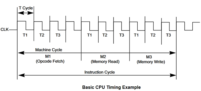
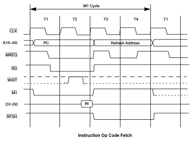
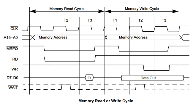
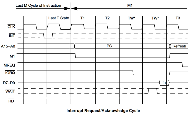
Z80 diagrams
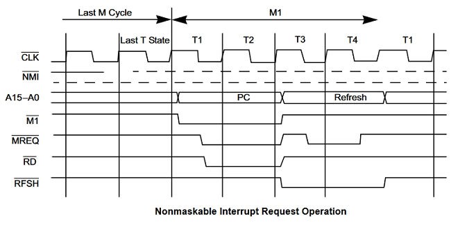
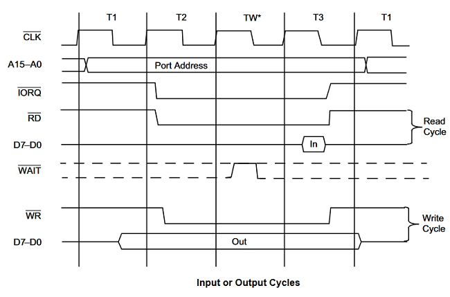
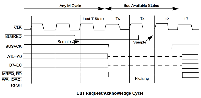
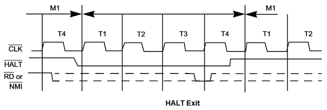
Here are some useful diagrams, including the Z80 pinout, timing diagrams, etc.
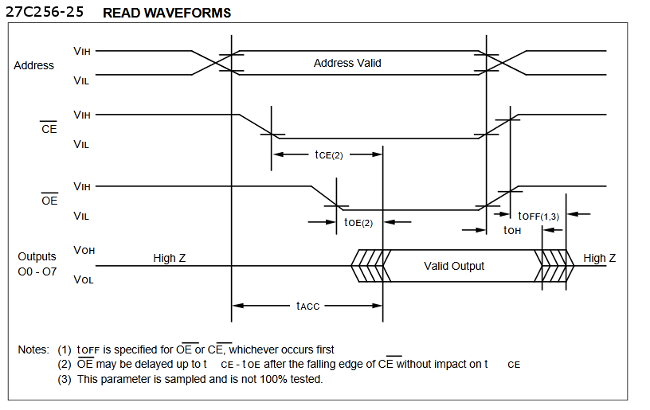
27C256 EPROM diagrams
Here are some useful diagrams, including pinout, timing, etc.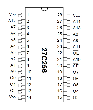
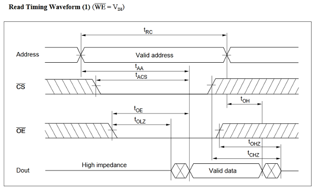
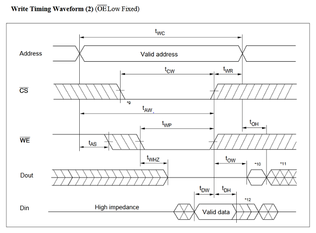
62256 RAM diagrams
Here are some useful diagrams, including pinout, timing, etc.