Electronic Circuits - interfacing with a Z80 microprocessor v6 (clock and interrupts)
My seb80 custom computer now has its own page here
This is version 6 of my Z80 interfacing project. My goal in this version was to introduce an oscillator clock, as well as experiment with the NMI and INT interrupts.
Previous versions:
Previous versions:
Version 6 introduces an oscillator clock and a manual NMI circuit (activated via push button) alongside the manual, push button NMI. To test both NMI and INT interrupts, I wrote three programs.
See the log below for program listings.
TP1 - test program for NMI
TP2 - test program for INT
TP3 - second test program for NMI
Log
day 1Wired up a 555 circuit.
I did it much faster than the last time I worked with a 555, probably because of the few hundred connections I've made for the Z80.
day 2
Replaced the last two 74F series chips with 74LS, to rely exclusively on the 74LS family of TTL logic ICs.
Broke a pin on one CPU and discovered that another one was faulty (internal short-circuit).
That means I'm down to two good CPUs.
Re-wired the manual clock ICs and introduced a switch which selects between manual clock and 555-driven clock.
This has allowed me for the first time to observe instruction timing on an oscilloscope.
day 3
Reset is now automatic. I used a simple RC circuit to make the RESET pin start low at power-on and reach 2V after a generous 0.8 seconds - giving enough low-level time for three clocks, ensuring a successful reset.
It will also feature a push button to allow manual reset as well, for the cases when clock is manual or just to reset more easily partway through program execution.
day 4
Designed a "generate NMI" button. I debounced it just like the clock button, to prevent multiple NMIs from being generated on a push.
Wrote TP1, the NMI test program.
address  bytes                mnemonic

0000                          ; TP1

0000                          ; test program for NMI

0000                          ;   loops while NMI routine has not run

0000                          ;   enters infinite loop after NMI routine runs

0000                          ;

0000   31 00 90               LD   SP,9000h    ; stack bottom (NMI needs stack)

0003   3E 00                  LD   A,0

0005   32 FF FF               LD   (0FFFFh),A  ; hasNmiRun := FALSE

0008                WAIT_NMI:                  ; do

0008   3A FF FF               LD   A,(0FFFFh)

000B   FE 00                  CP   0

000D   CA 08 00               JP   Z,WAIT_NMI  ; while !hasNmiRun

0010                AFTER_NMI:

0010   00                     NOP

0011   C3 10 00               JP   AFTER_NMI   ; infinite loop

0014   FF FF ..               DB 82 DUP (0FFh) ; pad up to NMI routine start

0066                NMI_ROUTINE:

0066   3E 01                  LD   A,1

0068   32 FF FF               LD   (0FFFFh),A  ; hasNmiRun := TRUE

006B   ED 45                  RETN             ; return from NMI
Program was verified successfully! Before NMI is generated, the CPU loops between 0008 and 000D. After NMI is generated, the CPU enters the infinite loop at 0010.
day 5
Changed all pull-up resistors in my design to 10k for consistency's sake.
I'm going to test INT interrupt signals with a bouncy push button. For fun, I will be able to see how many bounces each push generated.
Wrote TP2, the INT test program.
address  bytes                mnemonic

0000                          ; TP2

0000                          ; test program for INT

0000                          ;   infinite loop which reads a variable which holds

0000                          ;       a count of generated INT signals

0000                          ;   INT routine increments count variable

0000                          ;

0000   31 00 90               LD   SP,9000h    ; stack bottom (INT needs stack)

0003   21 0F F0               LD   HL,0F00Fh

0006   36 00                  LD   (HL),0      ; initialize counter

0008   ED 56                  IM   1           ; choose interrupt mode 1,

000A                                           ; which assumes that the

000A                                           ; interrupt handler is at 0038

000A   FB                     EI               ; enable interrupts

000B                READ_COUNT:

000B   21 0F F0               LD   HL,0F00Fh

000E   7E                     LD   A,(HL)      ; read INT count

000F   C3 0B 00               JP   READ_COUNT  ; infinite loop

0012   FF FF ...              DB 38 DUP (0FFh) ; pad up to INT handler start

0038                INT_HANDLER:

0038   21 0F F0               LD   HL,0F00Fh

003B   34                     INC   (HL)       ; count++

003C   ED 4D                  RETI             ; return from INT
Verified that the counter is incremented when an interrupt signal is raised.
Made a second test program for NMI, to count invocations.
address  bytes                mnemonic

0000                          ; TP3

0000                          ; a second test program for NMI

0000                          ;   infinite loop which reads a variable which holds

0000                          ;       a count of generated NMI signals

0000                          ;   NMI handler increments count variable

0000                          ;

0000   31 00 90               LD   SP,9000h    ; stack bottom (NMI needs stack)

0003   21 0F F0               LD   HL,0F00Fh

0006   36 00                  LD   (HL),0      ; initialize counter

0008                READ_COUNT:

0008   21 0F F0               LD   HL,0F00Fh

000B   7E                     LD   A,(HL)      ; read INT count

000C   C3 08 00               JP   READ_COUNT  ; infinite loop

000F   FF FF ...              DB 89 DUP (0FFh) ; pad up to NMI handler start

0066                NMI_HANDLER:

0066   21 0F F0               LD   HL,0F00Fh

0069   34                     INC   (HL)       ; count++

006A   ED 45                  RETN             ; return from NMI
Successfully observed NMI incrementing the counter variable.
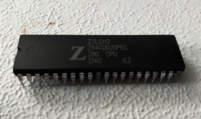
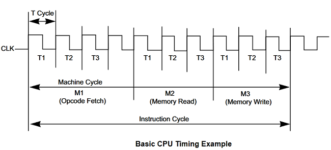
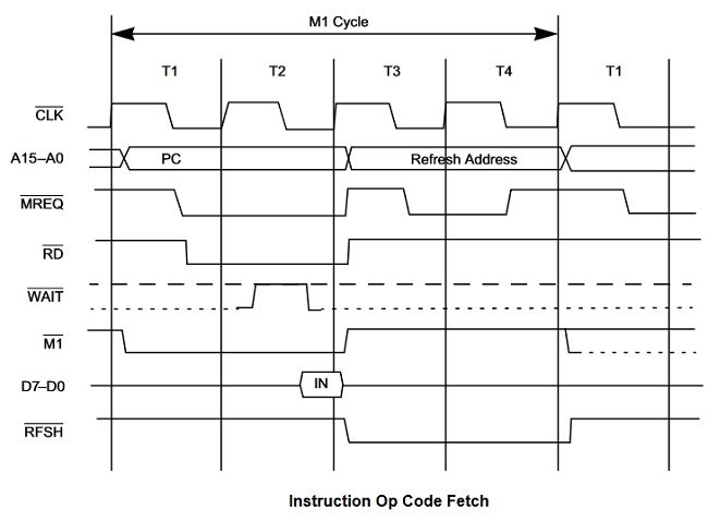
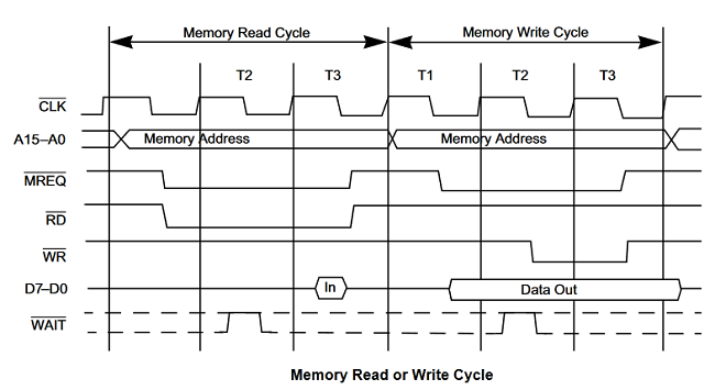
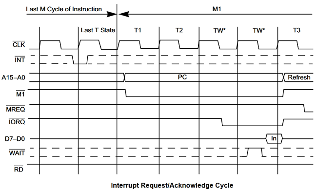
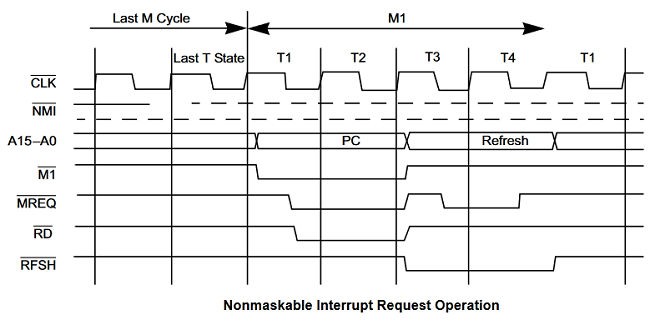
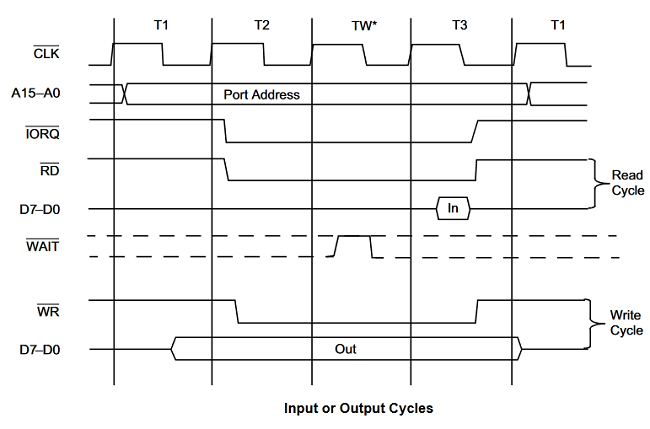
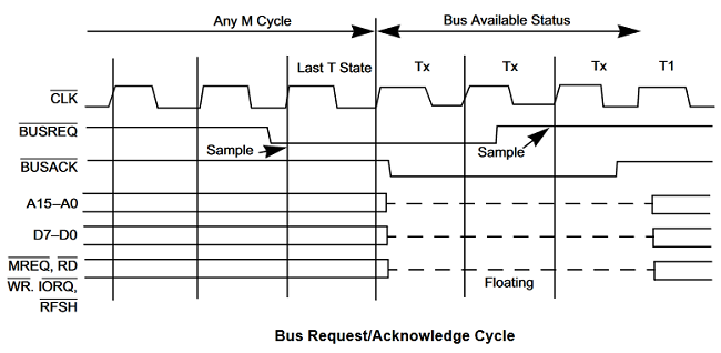
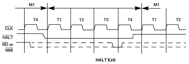
Z80 diagrams
Here are some useful diagrams, including the Z80 pinout, timing diagrams, etc.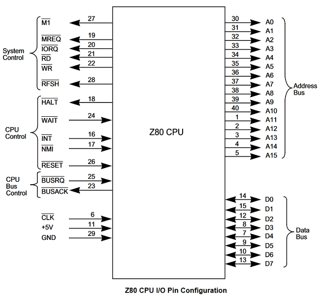
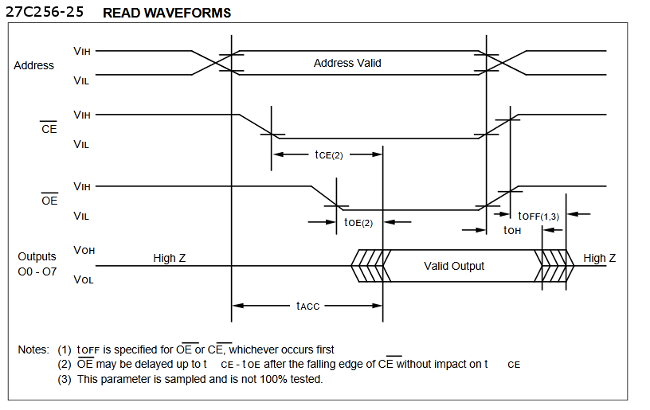
27C256 EPROM diagrams
Here are some useful diagrams, including pinout, timing, etc.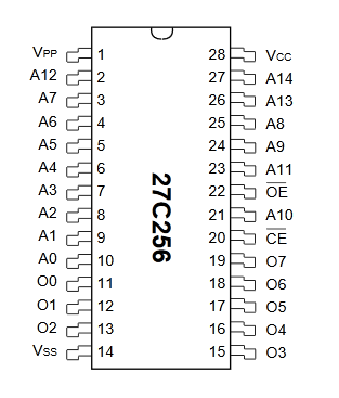
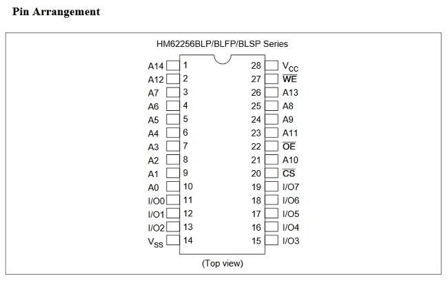
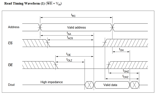
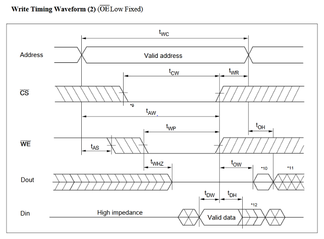
62256 RAM diagrams
Here are some useful diagrams, including pinout, timing, etc.