Electronic Circuits - interfacing with a Z80 microprocessor v1 (run NOPs)
My seb80 custom computer now has its own page here
Although most of the years I've spent coding in assembly language focused on the x86 CPU, the Z80 is near and dear to my heart. The reason for this is the computer (ZX Spectrum) that got me started in the world of software relied on a Z80 CPU.
A while back I created a game for the ZX Spectrum, during which I learned Z80 assembly language. The purpose here was to delve deeper, learn how it worked, and make this CPU do something interesting - but in the absence of a full-blown commercial computer built around it!
The Zilog Z80 is an 8-bit data, 16-bit address microprocessor released in the late 1970s. It had a variety of applications from personal computer main processor to sound processor in handheld gaming consoles, and was also used in graphing calculators, industrial control.
This is version 1 of my project, and I've kept it simple. My goal was to get a manually-clocked Z80 to execute the simplest instruction, NOP, while observing an incrementing PC (program counter) to ever higher addresses.
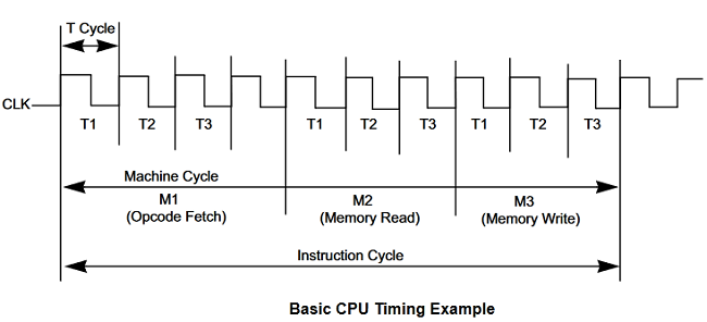
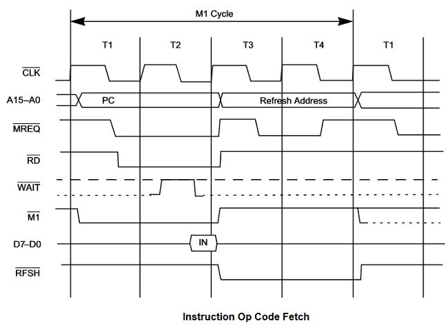
I wanted to perfectly match observed behaviour to Z80 specifications - such as CPU outputs to timing diagrams, clock cycle by clock cycle. This would serve as verification for my setup.
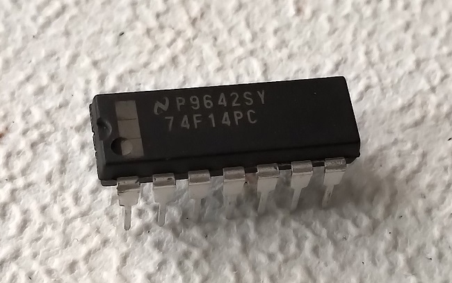
For clock and reset, I've used 74F series ICs because of their compatibility with the older 74 series and their more immediate availability.

Clock
A push button is used to generate clock signals. Its signal is cleaned up by a Schmitt trigger, to ensure clean edges. By default the clock is held high, since I discovered that when held low for a long time, the CPU can enter an undefined state.Reset
Another push button is used to bring the RESET line low (active) to reset the CPU. It too has its edges cleaned by a Schmitt trigger.Address lines
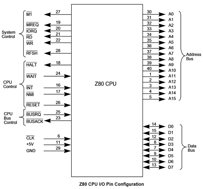
The first 8 of 16 address lines (A0-A7) are connected to LEDs, to allow easy observation of the incrementing PC (program counter) value. I've used 4.7k Ohm resistors (to LEDs), since A0-A7 are not really meant to drive anything.Data lines
All 8 data lines (D0-D7) are wired low. The CPU sees this as a NOP (value 0) instruction. This is great for testing because it allows the CPU to only require machine cycle 1 (M1), which is 4 clock cycles long. This is because no memory accesses are needed by NOP.Outputs
I've only sampled a few outputs (also via 4.7k Ohm resistors to LEDs) - enough to trace the CPU through the spec timing diagram of the 4-clock cycle M1.

Log
day 1Tried out a CMOS 4584 schmitt trigger IC (plus an inverter) to get some clean edges from a push button.
The 4584 did nothing until I gave it a pull-down resistor.
day 2
Connected all data pins to ground (00000000b = NOP) and first few data pins (D0-D7) to LEDs.
This is equivalent to the program:
0000 NOP
0001 NOP
0002 NOP
etc.
Note: RESET has to stay active (low) for at least 3 clocks, so while I hold down the RESET push button, I have to clock it a few times as well.
Issue: clock signal is dirty - it has to be much cleaner
Issue: address seems to be incrementing, but not cleanly... probably because of the dirty clock
Issue: sometimes the CPU freezes (clocking stops incrementing address)
Note: CPU enters a strange state (garbage on the address lines) if clock line stays low for too long. This may be related to its expectation of the clock line being high during a power down (when HALT is active) state.
day 3
Changed clock to be pulled high and with a capacitor I get much better (90% accurate) debouncing.
I also added an inverter in series with Schmitt and the CPU no longer locks up.
Address increments are not always clean; CPU seems to output junk every now and then.
day 4
Switched Schmitt from a 4584 to a 74HC14 and inverter from a 4069 to a 74F04.
Now the CPU increments the address cleanly, once every 4 clocks.
day 5
I tested without the inverter on the clock pin and it causes CPU to be erratic again, so I'll keep it on.
day 6
After much headache, I learned that timing diagrams graphs show voltage levels and NOT logical levels.
This cleared up confusion around active-low Z80 outputs.
day 7
Reorganized the board to create more space.
Added further LEDs for CPU outputs, clock, etc.s
day 8
Replaced 74HC14 with 74F14 (to match the inverter 74F04).
I also tried 7414 and that behaved strangely.
For now, I will keep using 74F14 and 74F04.
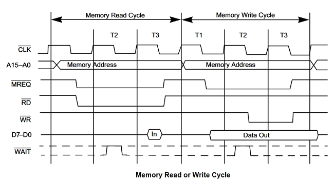
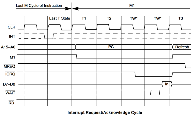
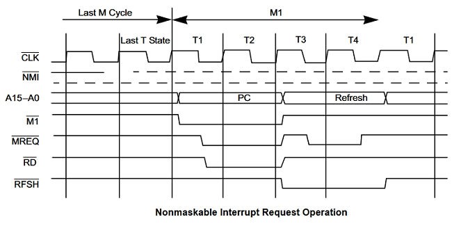
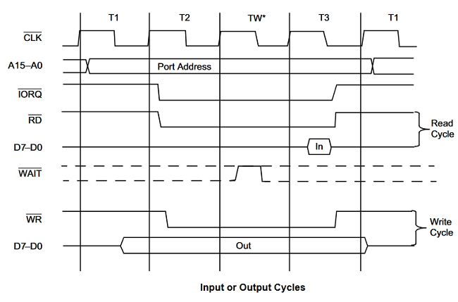
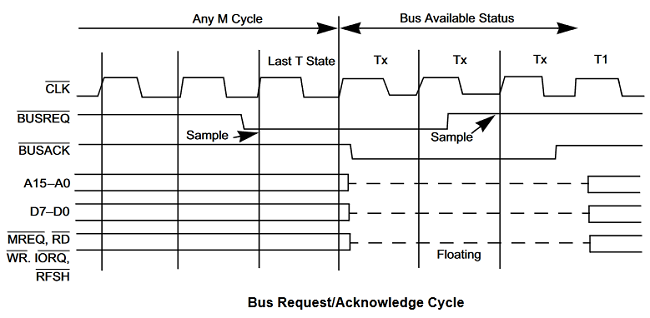
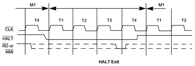
Z80 diagrams
Here are some useful diagrams, including the Z80 pinout.